Tuesday, December 17, 2013
Simple Self Oscillating Switching Converter Circuit Diagram

Monday, September 30, 2013
Preamplifier For Soundcard Circuit

Sunday, September 22, 2013
Non Contact Power Monitor circuit
Here is a simple non-contact AC power monitor for home appliances and laboratory equipment that should remain continuously switched-on. A fuse failure or power breakdown in the equipment going unnoticed may cause irreparable loss. The monitor sounds an alarm on detecting power failure to the equipment. The circuit is built around CMOS IC CD4011 utilising only a few components. NAND gates N1 and N2 of the IC are wired as an oscillator that drives a piezobuzzer directly. Resistors R2 and R3 and capacitor C2 are the oscillator components. The amplifier comprising transistors T1 and T2 disables the oscillator when mains power is available. In the standby mode, the base of T1 picks up 50Hz mains hum during the positive half cycles of AC and T1 conducts.
Circuit diagram:

Non-Contact Power Monitor circuit diagram
This provides base current to T2 and it also conducts, pulling the collector to ground potential. As the collectors of T1 and T2 are connected to pin 2 of NAND gate N1 of the oscillator, the oscillator gets disabled when the transistors conduct. Capacitor C1 prevents rise of the collector voltage of T2 again during the negative half cycles. When the power fails, the electrical field around the equipment’s wiring ceases and T1 and T2 turn off. Capacitor C1 starts charging via R1 and preset VR and when it gets sufficiently charged, the oscillator is enabled and the piezobuzzer produces a shrill tone. Resistor R1 protects T2 from short circuit if VR is adjusted to zero resistance.
The circuit can be easily assembled on a perforated/breadboard. Use a small plastic case to enclose the circuit and a telescopic antenna as aerial. A 9V battery can be used to power the circuit. Since the circuit draws only a few microamperes current in the standby mode, the battery will last several months. After assembling the circuit, take the aerial near the mains cable and adjust VR until the alarm stops to indicate the standby mode. The circuit can be placed on the equipment to be monitored close to the mains cable.
Wednesday, September 11, 2013
Simpled Solar Powered Lithium Ion Battery Charger Circuit

Monday, May 27, 2013
Simple ufo Detector Circuit Diagram

Note
# Use 3V power supply
# Click this to make UM66 music circuit
Friday, May 17, 2013
BA5406 Stereo Amplifier Circuit

Purpose of the Zobel network is to cut back oscillations and improve high frequency stability of the amplifier. Potentiometers R5 and R6 serves as the quantity control for the left and right channels. CapacitorsC4 and C8 couple the outputs of the amplifier to the speakers. C9 and C10 are noise filtering capacitors. C1 and C5 are bootstrap capacitors for the left and right channels.
Monday, May 13, 2013
25 Watt Audio Amplifier Circuit
 This is a 25 Watt basic power amp that was designed to be (relatively) easy to build at a reasonable cost. It has better performance than the standard STK module amps that are used in practically every mass market stereo receiver manufactured today. When I originally built this thing, it was because I needed a 25 Watt PC amp and did not want to spend any money. So I designed around parts I had in the shop.
 Parts:
R1 = 47K R2 = 4K7 R3 = 1K5 R4 = 47K R5 = 390R R6 = 470R R7 = 33K R8 = 150K R9 = 15K R10 = 27R R11 = 500R-1/2W R12 = 10R R13 = 10R R14 = 220R R15 = 220R R16 = 10R R17 = 8.2R-2W R18 = 22R-4W(wirewound) C1 = 470nF-63V C2 = 330pF-63V C3 = 470µF-63V C4 = 100nF-63V C5 = 470µF-63V C6 = 100nF-63V C7 = 100µF-25V C8 = 100nF-63V C9 = 10pF-63V C10 = 1µF-63V C11 = 100nF-63V Q1 = BC560C Q2 = BC560C Q3 = BC560C Q4 = BC560C Q5 = BC560C Q6 = BD140 Q7 = BD139 Q8 = IRF530 Q9 = IRF9530
Parts:
R1 = 3K3-1/2W C1 = 10nF-1000V C2 = 4700µF-50V C3 = 4700µF-50V C4 = 100nF-63V C5 = 100nF-63V D1 = 200V 8A Diode bridge D2 = 5mm. Red LED F2 = 3.15A Fuses with sockets F2 = 3.15A Fuses with sockets T1 = 220V Primary, 25 + 25V Secondary 120VA Mains transformer PL1 = Male Mains plug SW1 = SPST Mains switch
Notes:
* Can be directly connected to CD players, tuners and tape recorders. Simply add a 10K Log potentiometer (dual gang for stereo) and a switch to cope with the various sources you need. * Q6 & Q7 must have a small U-shaped heatsink. * Q8 & Q9 must be mounted on heatsink. * Adjust R11 to set quiescent current at 100mA (best measured with an Avo-meter connected in series to Q8 Drain) with no input signal. * A correct grounding is very important to eliminate hum and ground loops. Connect to the same point the ground sides of R1, R4, R9, C3 to C8. Connect C11 to output ground. Then connect separately the input and output grounds to power supply ground. * An earlier prototype of this amplifier was recently inspected and tested again after 15 years of use. Results, comments and pictures are shown here.
Friday, April 12, 2013
Flip Flop Led Circuit

555 Timer Touch Activated Alarm Circuit Diagram

Monday, April 8, 2013
How to Make a Light Activated Day Night Switch Circuit – Science Fair Project
At this condition the voltage at the inverting input will be higher than the reference at non inverting pin and the out put of the comparator will be low(~o V). When the LDR is illuminated ,its resistance drops and so do the voltage across it.Now the voltage at inverting input will be lower than that at non inverting input and the out put of the comparator goes high (~12 V). This makes transistor Q1 on and it drives the relay.As a result we get a relay switching according to the intensity of the light falling on the LDR.
Light Activated Switch Circuit Diagram with Parts List .

Notes.
- Adjust POT R1 to set the desired light intensity for switching the relay.For this illuminate the LDR with the desire intensity light.The relay will be either on or off.Adjust POT R1 slowly so that the state of the relay changes.That’s it.Now the circuit is set for the given intensity of light.
- Assemble the circuit on a good quality PCB or common board.
- You can use either a 12 V battery or a well regulated & filtered 12V DC mains operated power supply.
- The pin 5&6 (Balance & Balance/Strobe ) of IC LM311 are shorted to minimize the chance of oscillations.
- The pin out of LM311 is also given together with the circuit diagram.
Saturday, April 6, 2013
Power Saver Circuit Saving electricity

Because of the way it works is to reduce the magnitude from cosine curve AC current that will be read on the gauge kilometer. Device work if there is air conditioning load passes through a coil of wire sensors to measure the AC current which is being passed.
 |
| Power Saver Circuit |
9 Volt Power Supply Circuit Diagram Using IC 7809

Circuit showing a 9 volt power supply .
Here we have used a bridge rectifier and 7809 ic for making this circuit.Where the ic regulate the output to 9 v,1 A .This voltage every time constant.Are you interested ?
Component Required
Diodes
IN 4007 -4
Capacitor
C1 1000 MFD/16v
IC
7809
Transformer
9-0 V ,1 A
source by : http://www.electronics-circuits.in/2012/02/9-v-power-supply.html
Friday, April 5, 2013
100W BTL TDA2030 amplifier circuit
 |
| TDA2030 100W amplifier circuit |
Water Level Sensor Circuit Using LM1830 Single Chip
This is a water sensor circuit design using based on a Conductive Liquid Level Sensor, this single chip circuit is very compact and simple. This circuit is an ac excited fluid level sensor, which uses alternating current to provide biasing for the sensor probe to avoid electrolysis of the probes. This ac excitation makes the sensing probe has longer lifetime. This circuit can be useful for wide range of water or liquid level sensing and control such as radiators, beverage dispensers, washing machines, water softeners, irrigation, reservoirs, boilers, aquarium, or sump pumps
Many type of fluids are electrically conductive and can be detected using this liquid level sensor circuit: city water/ground water, sea water, chopper sulfate solution, weak acid, weak base, household ammonia, water and glycol mixture, wet soil, coffee, or fruit juices. Remember that most of fuel doesn’t conduct electricity, so this circuit can be employed as fuel level sensor/detector. This is the figure of the circuit.

If we look at its data sheet, this water level sensor circuit chip is best at 10-24 volt supply voltage. The absolute maximum voltage supply for this liquid level sensor chip is 28V, but remembers to always try to avoid this extreme condition to prevent damaging the chip.
In the first circuit, a basic low level warning application uses a LED to indicate the water level falls below the sensor. You can see the filter pin (9) is not connected, this means that the LED is actually blinking at sound frequency, but it’s fine since our eye response is slow enough to notice such high speed blinking. Since without filter capacitor at pin 9 the output give a square wave signal, you can easily replace the led with loud speaker as shown in the second circuit to give audio indication. If you need a TTL or CMOS level then you should use a filtering capacitor connected to pin 9 and use the open collector output to drive a pull up resistor connected to a voltage supply at desired voltage level. For water level control, or any conductive liquid level control, you can use a relay to activate a motor or valve to control the level. The third circuit show this kind of application, and the relay can be seen as liquid/water level switch. The optional resistor seen in the third circuit is an option for high voltage transient that often occurs in automotive environment, and you can omit it if there is no such possibility. [Circuits schematic diagram source: National Semiconductor Application Notes]
Thursday, April 4, 2013
Basic Principles of the LC resonance circuit

Simple 2 1 Surround Speaker System Circuit Diagram

Part List
| Component No: | Value | Usage |
| All C1 | 100MF | Grounding |
| All C2 | 100nF | Grounding |
| All C3 | 100nF | Grounding |
| All C4 | 100MF | Grounding |
| All C5 | 100MF | Feedback |
| All C6 | 100MF | Audio Coupling |
| All C7 | 220nF | Noise Grounding |
| All R1 | 1K | |
| All R2 | 10K ( Not 1K ) | |
| All R3 | 22K | |
| All R4 | 22K (Not 1K ) | |
| All RV1 | 100K | Volume Controlling |
| All D1 To D2 | IN4007 | Potential Breaking |
| U1 To U6 | TDA2030 | Amplification |
Applications
* 2.1 Surround Amplifier
* 2.1 Home Theater
Sunday, March 31, 2013
Pendulum Controlled Clock Circuit
Heres how to build a pendulum-controlled clock which can be made really accurate. Retro? - yes, but an interesting project all the same. Youll need a spare quartz clock which must be adapted by first isolating the two pads on the chip which lead to the coil. You then have to connect wires to these pads and feed them out through a hole in the case (see SILICON CHIP, December 1996, p38, for full instructions, or October 2001, p37, for brief notes.) Youll also need a spare battery driven pendulum from another, or the same, clock. As originally used, these pendulums are for appearance only and play no role in timekeeping. The salvaged unit should be mounted on a substantial vertical backboard. Youll find that the pendulum swings pretty fast and it must be slowed down by adding weights near the lower end. However, its not the mass of a pendulum that controls its rate - instead, its the distance from the support to the centre of mass that counts.
The aim is to make the pendulum operate so that it takes exactly 1s for a full "to and fro" swing - ie, 0.5s "beats". Fine adjustment on mine was made by adding an adjustable (up and down) weight to the pendulum rod. This consisted of a small G-clamp fabricated from a brass strip and held by a small screw.At the bottom end of the pendulum attach an inverted T-shape aluminium vane, about 10mm wide and as thin as possible. This should be painted black. This vane is used to trigger a photo-interrupter which is attached to the backboard. The lengths of the arms of the "T" are made so that when the pendulum swings one way, the interrupter triggers - ie, the light is no longer blocked. Conversely, when the pendulum swings the other way, the vane must continue to interrupt the light. This means that, with the pendulum swinging in 0.5s beats, we get a short pulse from the photo-interrupter at 1s intervals.
Circuit diagram:

Pendulum-Controlled Clock Circuit Diagram
This pulse is inverted by IC1a and inverted again by IC1b which then clocks IC2, a 4013 flipflop. IC2 alternately produces 1s-long pulses at its pin 12 & 13 outputs. These outputs are then fed to IC1c & IC1d respectively, where they are gated by the short pulses on pin 4 of IC1b. This produces two short pulses to drive the clock in alternate directions at 1s intervals. And thats all you need to drive the clock. Alternatively, this circuit could be a master clock and could be used to drive several slaves, all remaining in time. And model train enthusiasts could drill one or more holes in the vane to make their "railway" clocks run at what ever speed they need.
The circuit can be built on a small piece of strip board. Note that the photo-interrupter should be mounted with the photocell facing the backboard. This minimizes the risk of interference by ambient light. The photo-interrupter is available from Jaycar - Cat.ZD 1901. A footnote for horologists - if you have a clock with a Hipp butterfly escapement, you could rid yourself of the trailing arm and contact arrangement and replace it with a vane and photo-interrupter set so that as the arc of the swing becomes too small, a pulse is missed. This could then be detected by a 555 missing pulse detector circuit which would then energize the impulsing magnet.
Author: A.J Lowe - Copyright: Silicon Chip Electronics
Saturday, March 30, 2013
10 Watt Stereo Amplifier Circuit Using TDA2009A

Friday, March 29, 2013
Load Independent Output Corrected Inverter Circuit Discussed
The circuit was requested to me by one of my friends Mr.Sam, whose constant reminders prompted me to design this very useful concept for inverter applications.
The load independent/output corrected or output compensated inverter circuit explained here is quite on a concept level only and has not been practically tested by me, however the idea looks feasible because of its simple design.
If we look at the figure we see that the entire design is basically a simple PWM generator circuit built around the IC 555.
We know that in this standard 555 PWM design, the PWM pulses can be optimized by changing the ratio of R1/R2.
This fact has been appropriately exploited here for the load voltage correction application of an inverter.
An opto-coupler made by sealing an LED/LDR arrangement has been used, where the LDR of the opto- becomes one of the resistors in the PWM "arm" of the circuit.
The LED of the opto coupler is illuminated through the voltage from the inverter output or the load connections.
The mains voltage is suitably dropped using C3 and the associated components for feeding the opto LED.
After integrating the circuit to an inverter, when the system is powered (with suitable load connected), the RMS value may be measured at the output and the preset P1 may be adjusted to make the output voltage just suitable enough for the load.
This setting is probably all that would be needed.
Now suppose if the load is increased, the voltage will tend to fall at the output which in turn will make the opto LED intensity decrease.
The decrease in the intensity of the LED will prompt the IC to optimize its PWM pulses such that the RMS of the output voltage rises, making the voltage level also rise up to the required mark, this initiation will also affect the intensity of the LED which will now go bright and thus finally reach an automatically optimized level which will correctly balance the system load voltage conditions at the output.
Here the mark ratio is primarily intended for controlling the required parameter, therefore the opto should be placed appropriately either to the left or the right arm of the shown PWM control section of the IC.
The circuit can be tried with the inverter design shown in this article.

R1 = 330K
R2 = 100K
R3, R4 = 100 Ohms
D1, D2 = 1N4148,
D3, D4 = 1N4007,
P1 = 22K
C1, C2 = 0.01uF
C3 = 0.33uF/400V
OptoCoupler = Homemade, by sealing an LED/LDR face to face inside a light proof container.
Thursday, March 28, 2013
Simple AudioTone Control Circuit
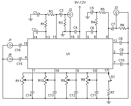
Simple AudioTone Control Circuit Part List
C1, C3, C5, C7, C15, C16 2.2uf Electrolytic Capacitor
C2, C6 0.05uF Ceramic Disc Capacitor
C4 0.22uF Disc Capacitor
C8, C10 0.015uF Ceramic Disc Capacitor
C9 100uF Electrolytic Capacitor
C11, C12, C13, C14 0.1uF Ceramic Disc Capacitor
R1, R4 10K 1/4W Resistor
R2, R5 33K 1/4W Resistor
R3, R6 4.7K 1/4W Resistor
R7 2.2K 1/4W Resistor
R8, R9, R10, R11 50K Linear Pot
U1 TDA1524A Tone Control IC
S1 SPST Switch
J1, J2, J3, J4 4 RCA Jacks
MISC Board, Wire, Knobs, 18 Pin Socket
NOTES
- S1 is a contour control. Volume is controlled by R11. Balance is controlled by R10. R9 and R8 control bass and treble, respectivly.
- J1 is the left input, J4 is the right input. J2 is the left output, J3 is the right output.
- The circuit is designed to accept line level or mic level inputs. if you are going to be using a stronger signal, a voltage divider will be necessary to cut it down to proper levels.
- You can, of course, skip J1-J4 if you plan to integrate this circuit into another.