Showing posts with label amplifier. Show all posts
Showing posts with label amplifier. Show all posts
Thursday, January 9, 2014
Audio Amplifier
This audio amplifier circuit delivers up to 200 W of top-class quality for loudspeaker from 4 to 16 ohm. Operating voltage is between 24 and 36 V, max 5 A. The frequency response is from 20 to 20000 Hz.
Please take special care that the transistors and the IC’s have been fixed firmly and solely one or two separated cooling elements with sufficient dimensions for this purpose (thermal resistance < 1K/W).
Please take special care that the transistors and the IC’s have been fixed firmly and solely one or two separated cooling elements with sufficient dimensions for this purpose (thermal resistance < 1K/W).
200W Power Amplifier circuit diagram

Doing so it is necessary to mount the transistors and the IC’s insulated (with mica washes and plastic nipple). Please make sure before first operation that the transistors and the IC’s really do not have any electrical connection towards the cooling plate! The transistors have to be placed plane and firmly onto the cooling element! It is of extraordinary importance with this high-power amplifier that there is a considerable heat dissipation. The already mounted cooling element should be situated in a well ventilated case.
The PSU should be sufficiently powerful, power consumption of the amplifier may increase up to 5A. In case of using an unstabilised power supply. It is advisable to place a transformer of max 28V.
The amplifier will the show approx. 120W at a 4-Ohm loudspeaker, for it no-load voltage of the power supply will not be to high. If it is desired to use complete power, it is necessary to place a stabilised power supply with approx. 36V 5A. No-load voltage should not pass over 44V!
The cables leading the current supply and to the loudspeakers should have at least a cross section of min. 1.5 mm^2. The connected loudspeaker have to be equiped according to the high output power and should not have a lower impedance as 4 Ohm! With lower connection impedance and short circuit within the loudspeaker wiring, the transistors will be destructed.
The amplifier has an input sensitivity of approx. 500 … 800 mV. Therefore, it is possibile to connect directly at the amplifier tape decks, tuners, etc. In case there are connected signal sources with lower output voltage, it is necessary to pre-connect a preamplifier. Then it will alse be posible to connect microphones, etc.
200W audio amplifier PCB


Audio power amplifier components
IC1, IC2 = 2 IC’s TDA2030T1, T3 = 2 transistors KT818 or BD708
T2, T4 = 2 transistors KT819 or BD705
C1, C2, C3, C4, C7 = 5 capacitors 150 nF
C5 = 1 elca 10uF 63V
C8 – 1 capacitor 1.8 nF
R1, R7, R9 = 3 resistances 100K
R2, R3, R10, R11 = 4 resistances 2.2 Ohm
R4, R5 = 2 res. 2K
R6, R8 = 2 res. 1 Ohm
R12, R13 = 2 res. 2 res. 3.3K
D1…D4 = 1N4001, 1N4002, 1N4003
1 PCB board approx 56×51 mm
Friday, May 17, 2013
BA5406 Stereo Amplifier Circuit

In the circuit diagram shown, BA5406 is configures to deliver 5×2 watts into 4 ohm loudspeakers at a supply offer voltage of 9 volts. Capacitor C3 is a power supply filter capacitor. C11 and C12 are input DC decoupling capacitors for the left and right channels. C3 and R2 forms a Zobel network for the left output whereas C6 & R3 forms identical for the correct channel.
Purpose of the Zobel network is to cut back oscillations and improve high frequency stability of the amplifier. Potentiometers R5 and R6 serves as the quantity control for the left and right channels. CapacitorsC4 and C8 couple the outputs of the amplifier to the speakers. C9 and C10 are noise filtering capacitors. C1 and C5 are bootstrap capacitors for the left and right channels.
Purpose of the Zobel network is to cut back oscillations and improve high frequency stability of the amplifier. Potentiometers R5 and R6 serves as the quantity control for the left and right channels. CapacitorsC4 and C8 couple the outputs of the amplifier to the speakers. C9 and C10 are noise filtering capacitors. C1 and C5 are bootstrap capacitors for the left and right channels.
Monday, May 13, 2013
25 Watt Audio Amplifier Circuit
 This is a 25 Watt basic power amp that was designed to be (relatively) easy to build at a reasonable cost. It has better performance than the standard STK module amps that are used in practically every mass market stereo receiver manufactured today. When I originally built this thing, it was because I needed a 25 Watt PC amp and did not want to spend any money. So I designed around parts I had in the shop.
 Parts:
R1 = 47K R2 = 4K7 R3 = 1K5 R4 = 47K R5 = 390R R6 = 470R R7 = 33K R8 = 150K R9 = 15K R10 = 27R R11 = 500R-1/2W R12 = 10R R13 = 10R R14 = 220R R15 = 220R R16 = 10R R17 = 8.2R-2W R18 = 22R-4W(wirewound) C1 = 470nF-63V C2 = 330pF-63V C3 = 470µF-63V C4 = 100nF-63V C5 = 470µF-63V C6 = 100nF-63V C7 = 100µF-25V C8 = 100nF-63V C9 = 10pF-63V C10 = 1µF-63V C11 = 100nF-63V Q1 = BC560C Q2 = BC560C Q3 = BC560C Q4 = BC560C Q5 = BC560C Q6 = BD140 Q7 = BD139 Q8 = IRF530 Q9 = IRF9530
Parts:
R1 = 3K3-1/2W C1 = 10nF-1000V C2 = 4700µF-50V C3 = 4700µF-50V C4 = 100nF-63V C5 = 100nF-63V D1 = 200V 8A Diode bridge D2 = 5mm. Red LED F2 = 3.15A Fuses with sockets F2 = 3.15A Fuses with sockets T1 = 220V Primary, 25 + 25V Secondary 120VA Mains transformer PL1 = Male Mains plug SW1 = SPST Mains switch
Notes:
* Can be directly connected to CD players, tuners and tape recorders. Simply add a 10K Log potentiometer (dual gang for stereo) and a switch to cope with the various sources you need. * Q6 & Q7 must have a small U-shaped heatsink. * Q8 & Q9 must be mounted on heatsink. * Adjust R11 to set quiescent current at 100mA (best measured with an Avo-meter connected in series to Q8 Drain) with no input signal. * A correct grounding is very important to eliminate hum and ground loops. Connect to the same point the ground sides of R1, R4, R9, C3 to C8. Connect C11 to output ground. Then connect separately the input and output grounds to power supply ground. * An earlier prototype of this amplifier was recently inspected and tested again after 15 years of use. Results, comments and pictures are shown here.
Saturday, April 13, 2013
1 W Home Stereo Amplifier Rise
This is a one watt dwelling stereo amplifier module project the use of the KA2209 IC from Samsung, which is equal to the TDA2822. It functions from three-12V DC & will work from a battery because the dormant current drain is low. It requires no warmth sink for standard use. The enter & output are both floor referenced. Maximum output will most probably be bought with a 12V energy supply & 8 ohm speaker, on the other hand it is suitable for driving headphones from a provide as low as threeV.
The Specifications of the house stereo amplifier :
The Specifications of the house stereo amplifier :
D.C. input : 3 – 12 V at 200 – 500 mA max
Idle current : approx. 10 mA
Power output : > 1 Watt max. 4-8 ohms, 12V DC
Freq. Resp. : approx. 40 Hz to 200 okayHz, 8 ohm, G=10
THD : < 1 % @ 750 mW, 4-8 ohm, 12V
Gain : approx. x10 (20 dB) OR x100 (40dB)
S/N ratio : > eighty dB, G = 20 dB
Sensitivity : < three00 mV, G = 20 dB
Input Impedance : approx. 10 ok ohm
Description
The achieve is adjustable from ten to one hundred, i.e. twenty to 40 dB. Start with remarks resistors R1 and R3 of 1k ohm, this could give a gain of ten which should be adequate for many applications. In case you need more gain, you can eliminate resistors R1 and R3.This will provide a gain of about 100, or 40 dB.The enter attenuation can additionally be adjusted by means of the potentiometer which can be utilized as a quantity keep an eye fixed on. The IC achieve ought to be okept as low as important to perform full output, with the in put potentiometer and your sign source at maximum.

Voltage Gain = 1+ R1/R2 = 1+R3/R4, however the utmost acquire without a outdoor comments is about a hundred, or fortydB. (GdB = 20log Gv)
This will okayeep the signal to noise ratio as high as feasible. Additional acquire supplied via the amplifier will cut again the S/N ratio by using a identical quantity, since the input noise figure is continuing. Other values for R1 and R3 of between 1k and 10k ohm can be used if an intermediate acquire level is necessary.
This will okayeep the signal to noise ratio as high as feasible. Additional acquire supplied via the amplifier will cut again the S/N ratio by using a identical quantity, since the input noise figure is continuing. Other values for R1 and R3 of between 1k and 10k ohm can be used if an intermediate acquire level is necessary.
If riding a pair of headphones, you too can want a a hundred ohm resistor in sequence with each output to lower again the output stage, relying on headphone impedance & sensitivity. Make positive you begin with the quantity proper all the way down to test. Numerous headphones is additionally pushed from the amplifier in the experience you wish, considering most headphones have as a minimum sixteen ohm impedance, or extra frequently 32 ohm.
There are only some out of doors phases, the IC comprises many of the essential circuitry. R1,R2 and R3,R4 are the feedback resistors. C1 offers power provide decoupling. C2 and C3 are the enter coupling capacitors, which block any DC that might-be existing on the enters. C4,C5 block DC within the feed again circuit from the inverting enters, and C6,C7 are the output coupling capacitors. C8, R5 and C9,R6 act as Nobel networks providing a excessive frequency load to handle stability at frequencies the place loud speaker inductive reactant may turn out to be extreme. The pot offers adjustable input degree attenuation.

Friday, April 12, 2013
9 VOLT HEADPHONE AMPLIFIER NE5534 SCHEMATIC DIAGRAM
9 VOLT HEADPHONE AMPLIFIER NE5534 SCHEMATIC DIAGRAM
The NE5532 is a very convenient package of two 5534s in one 8-pin devices with internal unity-gain compensation, as there are no spare pins. The 5534/2 is a low-distortion, low-noise device, having also the ability to drive low-impedance loads to a full voltage swing while maintaining low distortion. Furthermore, it is fully output short-circuit proof. Therefore, this circuit was implemented with a single NE5532 chip forming a pair of stereo, inverting amplifiers, having an ac gain of about 3.5 and capable of delivering up to 3.6V peak-to-peak into a 32 Ohm load (corresponding to 50mW RMS) at less than 0.025% total harmonic distortion (1kHz & 10kHz).
I have Used it with Sennheiser 465s and achieved ear-splitting volume. The amplifier is ideal as a booster for power-conserving stereo sources Such as portable CD players and for interfacing with passive EQ networks Such as tone controls or a headphone acoustic simulator.
Continue Reading..
The NE5532 is a very convenient package of two 5534s in one 8-pin devices with internal unity-gain compensation, as there are no spare pins. The 5534/2 is a low-distortion, low-noise device, having also the ability to drive low-impedance loads to a full voltage swing while maintaining low distortion. Furthermore, it is fully output short-circuit proof. Therefore, this circuit was implemented with a single NE5532 chip forming a pair of stereo, inverting amplifiers, having an ac gain of about 3.5 and capable of delivering up to 3.6V peak-to-peak into a 32 Ohm load (corresponding to 50mW RMS) at less than 0.025% total harmonic distortion (1kHz & 10kHz).
I have Used it with Sennheiser 465s and achieved ear-splitting volume. The amplifier is ideal as a booster for power-conserving stereo sources Such as portable CD players and for interfacing with passive EQ networks Such as tone controls or a headphone acoustic simulator.
Tuesday, April 9, 2013
1W BTL Audio Amplifier
The TDA8581(T) from Philips Semiconductors is a 1-watt Bridge Tied Load (BTL) audio power amplifier capable of delivering 1 watt output power into an 8-Wload at THD (total harmonic distortion) of 10% and using a 5V power supply.
The schematic shown here combines the functional diagram of the TDA8551 with its typical application circuit. The gain of the amplifier can be set by the digital volume control input. At the highest volume setting, the gain is 20 dB. Using the MODE pin the device can be switched to one of three modes: standby (MODE level between Vp and Vp–0.5 V), muted (MODE level between 1 V and Vp–1.4 V) or normal (MODE level less than 0.5 V). The TDA8551 is protected by an internal thermal shutdown protection mechanism. The total voltage loss for both MOS transistors in the complementary output stage is less than 1 V.
1 Watt BTL Audio Amplifier Circuit diagram:

Using a 5-V supply and an 8-W loudspeaker, an output power of 1 watt can be delivered. The volume control has an attenuation range of between 0 dB and 80 dB in 64 steps set by the 3-state level at the UP/DOWN pin: floating: volume remains unchanged; negative pulses: decrease volume; positive pulses: increase volume Each pulse at he Up/DOWN pin causes a change in gain of 80/64 = 1.25 dB (typical value).
When the supply voltage is first connected, the attenuator is set to 40 dB (low volume), so the gain of the total amplifier is then –20 dB. Some positive pulses have to be applied to the UP/DOWN pin to achieve listening volume. The graph shows the THD as a function of output power. The maximum quiescent current consumption of the amplifier is specified at 10 mA, to which should be added the current resulting from the output offset voltage divided by the load impedance.
Friday, April 5, 2013
100W BTL TDA2030 amplifier circuit
TDA2030 amplifier circuit using the BTL system has a 100W output power and voltage of +15 V,-15V 0. Amplifier circuit you can see below.
 |
| TDA2030 100W amplifier circuit |
Tuesday, April 2, 2013
Guitar amplifier pioneer Jim Marshall dies aged 88
 LONDON (Reuters) - Jim Marshall, dubbed the "Lord of Loud" for his pioneering work on guitar amplifiers used by some of the greatest names in rock music, has died aged 88.
A spokeswoman for the company he founded said he passed away in Milton Keynes, southeast England, on Thursday morning. She could not confirm reports that he had been suffering from cancer and had a series of strokes.
"It is with profound sorrow that we announce the passing of our beloved founder and leader for the past 50 years, Jim Marshall," said a statement on his companys website.
"While mourning the Guvnor though, we also salute a legendary man who led a full and truly remarkable life."
Tributes poured in for a man credited with helping to shape the sound of guitar rock.
"The news of Jim Marshall passing is deeply saddening," former Guns N Roses guitarist Slash said in a message on Twitter. "R & R will never be the same w/out him. But, his amps will live on FOREVER!"
His company said in a written tribute: "Your memory, the music and joy your amps have brought to countless millions for the past five decades and that world-famous, omnipresent script logo that proudly bears your name will always live on."
TOWNSHEND, HENDRIX AMONG EARLY CLIENTS
Marshall is revered as one of the four forefathers of rock music equipment along with Leo Fender, Les Paul and Seth Lover.
Born in London in 1923, he started out as a drummer before going into business and founding Marshall Amplification in 1962.
In around 1960, a young Pete Townshend, later lead guitarist for The Who, first suggested to Marshall that he expand his music shop to sell guitars and amplifiers as well as drums.
According to an interview Marshall gave several years ago, the London store quickly turned into a "rocknroll labour exchange", and Marshall hired an engineer employed by a record label to help him build prototype amplifiers.
Marshall rejected the first five attempts but was happy with the sound of the 6th -- he received 23 orders for the new equipment on the first day alone.
Legendary musicians including Jimi Hendrix and Eric Clapton were among the early Marshall amp users.
When Hendrix walked into the store, Marshall recalled thinking to himself: "Bloody hell, heres another American guitarist wanting something for nothing."
But the guitarist paid the full price for everything he purchased without delay.
Marshall was awarded an OBE honor for services to the music industry and to charity, and he has donated millions of pounds to "worthy causes", according to his website.
They included the Royal National Orthopaedic Hospital in Stanmore where he was reportedly treated for tuberculosis as a child.
(Reporting by Mike Collett-White, Editing by Christine Kearney)
© Thomson Reuters 2012 All rights reserved.
Source:http://ca.reuters.com/article/entertainmentNews/idCABRE8340M220120405?pageNumber=2&virtualBrandChannel=0&sp=true
6 5W audio power amplifier

This amplifier circuit based on the ic, and the use here is that where ic STK4017 IC has output power of 6.5 watts with the impedance 8Ohm. Minimum required supply voltage and maximum 20Volt 35 Volt DC.Component
R1 = 100K
R2 = 2K7
R3 = 27R
C1 = 22uF
C2 = 100uF
C3 = 100uF
C4 = 100uF
C5 = 100uF
C6 = 47uF
C7 = 330uF
C8 = 100uF
U1 = STK4017
Besides using STK4017 ic, ic and can use that I mentioned the following:
STK4019
STK4021
STK4023
STK4025
Monday, April 1, 2013
BA1404 Transmitter with UPC1651RF Amplifier
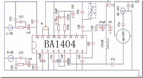
BA1404
transmitter includes onboard RF amplifier for increased transmitting
range. Operating voltage range is 1-3V, the circuit contains FM stereo
mixer, 38KHZ oscillator, FM modulator and high-frequency amplifier
monolithic integrated circuit. As the electronic newspaper BBS there
are many users requiring detailed information on the FM stereo
transmitter, so I re-collect the relevant information on the simple
discrete, merge, integrated FM stereo transmitter experiment, that
BA1404 with μpc1651 mix of the most easy to make and debug, and very
high frequency stability (relative to the previous circuit BA1404),
transmission power is increased by UPC1651RF amplifier.
Class T 30 watt amplifier Dayton
Dayton Audios DTA-1 has the hub of a serious player into a really portable package. A group-T imperfection lets the DTA-1 crop imaging, dynamics, and sound quality so as to rivals tube amps. Up to 15 watts for every channel is on tap to endorse bookshelf speakers.
 |
| Dayton Audio DTA-1 Class T Digital AC/DC Amplifier 15 |
- Palm-size course group-T 30 watt amplifier
- Battery otherwise AC powered-power supply integrated-instead of picture perfect portability
- 88% Amp efficiency for longer battery life
- senior sound quality
Saturday, March 30, 2013
10 Watt Stereo Amplifier Circuit Using TDA2009A
This is a design circuit for amplifier. This amplifier circuit has a power of 10 watts. This amplifier circuit is very suitable to apply to your car audio. This amplifier is using IC TDA2009A, as amplifier power. To avoid excessive heat in the IC using some heat sink compound between the heat sink & the IC. C1 & C2 is the input coupling capacitor and blocks DC, as well as C10 & C11 which is the output capacitor Kopel, and C6 & C7 which blocks the DC from the feedback loop. R1/R2 (and R3/R4) set the level of feedback. This is the figure of the circuit.

Get together with 1 (R1/R2) = 68 or 37 dB. C8/R5 (and C9/R6) provides high frequency stability where loudspeaker inductive reactance load can become excessive. C4 and C5 provide power decoupling or filtering. Absolute maximum supply voltage is 28V for the amplifier.
Thursday, March 28, 2013
High Fidelity Stereo Power Amplifier Circuit
This is a design circuit for audio power amplifier design utilizing the LM4702. This is a complete circuit for power amplifier design. This circuit has high quality circuit board layouts, the LM4702 power amplifier driver requires careful consideration. A good place to start is with the ground and power circuits design layout. This is the figure of the circuit;

Star connections for ground and power are always a good practice for audio circuit board layouts. A star connection is where there are individual traces from each component in the circuit that return to a central point. Notice how all the ground traces converge at the left side of the board, near Rs1 and Rs2, and connect to the two ground pins in the center of the power connector. The ground traces that connect to the right and left output jacks also converge at the center of the star ground which is the center of the power connector where the two ground pins are located.
[Circuit source: National Semiconductor Notes]
Wednesday, March 27, 2013
4 X 15 Watt Mini Power Amplifier
A lot of electronic circuits in the domain of audio amplifiers are already been published here. This circuit is a little different because it is a four channel amplifier. Each channel of this amplifier can deliver an output of 15Watts into a 4 ohm speaker. The amplifier can be operated from a single 12V DC supply and this makes it possible to use this amplifier in car audio applications too.
Circuit diagram :

4 X 15 Watt Mini Power Amplifier
The circuit is based on the 15W BTL X 2 channel audio power amplifier IC TA8215 from Toshiba. Even though chip is specifically designed for car audio applications it can be also used for home audio applications. Two TA8215 ICs are used here in order to obtain a 4 channel amplifier system. The circuit is designed almost exactly as per the application diagram in the ICs datasheet. Pins 7 and 19 are the Vcc pins of the ICs internal integrated power amplifier stages and these pins are connected to the positive supply. Pin 9 is the Vcc pin for ICs internal preamplifier and it is also connected to the positive supply. Pins 13 and 14 are the internal power amplifiers ground pins and they are tied together and connected to the ground.
The internal preamplifier’s ground pin (pin5) is connected to the common ground through a 10 Ohm resistor which makes the input ground separated from the common ground by a resistance of 10 ohms and this improves the noise rejection. The 100uF capacitor works as a power supply de-coupler. The resistor networks connected to the output lines of each amplifier improves the high frequency stability. The variable resistors (R3, R4, R12 and R13) works as the volume controller for the corresponding channels.
Notes :
- Assembling the circuit on a good quality PCB is a must for obtaining optimum sound quality.
- Use 12V DC for powering the circuit.
- The ICs must be fitted with adequately sized heat sinks.
- R3, R4, R12 and R13 serves as volume controllers.
- K1 to K4 can be 4 Ohm, 20W speakers.
- This amplifier circuit can be used in a variety of applications such as car audio systems, home theater systems, personal audio systems, public address systems etc. link
Tuesday, March 26, 2013
18W Car Stereo Amplifier Rise
This automobile stereo amplifier project is a class AB audio power amplifier using the Hitachi HA13118 module. It not only can be used in automobile application but also in any transportable or home amplifier process. It is simple to construct & has a maximum of outside parts. The module has a high power output from a low voltage supply using the bridge tied load system, & a high gain of 55dB.
This project will be useful in applications where the input signal is a low level, without requiring the use of a separate pre-amplifier. This IC module has a built in surge protection circuit, thermal shutdown circuit, ground fault protection circuit & power supply fault protection circuit making it reliable.
This project will be useful in applications where the input signal is a low level, without requiring the use of a separate pre-amplifier. This IC module has a built in surge protection circuit, thermal shutdown circuit, ground fault protection circuit & power supply fault protection circuit making it reliable.
The Specifications of this project
D.C. Input : 8 – 18V at 1-2 A
Power output : 18W maximum, 4 ohm load, 18V DC supply
S/N ratio : > 70 dB
THD : < 0.2% @ 1W
Freq. Response : ~ 30 Hz to 30 kHz, –3 dB
Input level : < 25 mV, for full output (G > 50dB)
Input Impedance : ~ 30 k ohm
D.C. Input : 8 – 18V at 1-2 A
Power output : 18W maximum, 4 ohm load, 18V DC supply
S/N ratio : > 70 dB
THD : < 0.2% @ 1W
Freq. Response : ~ 30 Hz to 30 kHz, –3 dB
Input level : < 25 mV, for full output (G > 50dB)
Input Impedance : ~ 30 k ohm
The supply voltage necessary for this project is 8 -18V DC, at least one to two Amps. Maximum output power will only be obtained with a power supply of 18V at greater than two A, using a four ohm speaker. The power supply ought to be well filtered to reduce mains hum, a regulated supply will reduce noise even further. Additional filtering is unnecessary if operating from a battery supply.
Circuit Diagram Description
Most of the circuitry is contained within the amplifier module. C10 is the input coupling capacitor and blocks DC from the input. C11 bypasses any RF which may be present at the input. C1 & C2 provide an AC ground for the inverting inputs of the IC. R1/C7 and R2/C8 provide a high frequency load for stability with difficult speakers. C five & C six provide bootstrap feedback for the IC. C9 & C12 provide power supply filtering.
Most of the circuitry is contained within the amplifier module. C10 is the input coupling capacitor and blocks DC from the input. C11 bypasses any RF which may be present at the input. C1 & C2 provide an AC ground for the inverting inputs of the IC. R1/C7 and R2/C8 provide a high frequency load for stability with difficult speakers. C five & C six provide bootstrap feedback for the IC. C9 & C12 provide power supply filtering.

An externally mounted logarithmic potentiometer of between 10k ohm and 50k ohm, is used depending on the desired input impedance. The impedance ought to be keep as high as feasible for a guitar amp, unless using a separate pre-amp. Make sure-that the heat sink is mounted to the module.

Subscribe to:
Posts (Atom)